Difference between revisions of "How to interface with two 16-bit Flash parts working as a single 32-bit Flash in EDK 12.1 using XPS MCH EMC"
From steamWiki
| Line 7: | Line 7: | ||
----- | ----- | ||
<br /> | <br /> | ||
| − | # Create | + | # Create a standard EDK project. |
| + | # Add an XPS_MCH_EMC Core. In this case, I have named it Flash_Mem. | ||
## Open the Properties sheet, navigate to the User tab and ensure that the Common properties match those shown below. | ## Open the Properties sheet, navigate to the User tab and ensure that the Common properties match those shown below. | ||
| − | ## | + | ##: [[File:Xps_mch_emc-prop-user-common.png]] |
| − | + | ## Now ensure that the Bank 0 properties match those shown below. | |
| + | ##: [[File:Xps_mch_emc-prop-user-bank0.png]] | ||
| + | ## Leave all other Properties as they are. Most are ignored. | ||
| + | # Add a UTIL_BUS_SPLIT Core. In this case I have named it Flash_A_Bus_Split. Ensure that the properties match those shown below. | ||
| + | #:: [[File:Util_bus_split-prop-user-all.png]] | ||
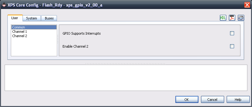
| + | # Add an XPS_GPIO Core. In this case I have called it Flash_Rdy. | ||
| + | ## Open the Properties sheet, navigate to the User tab and ensure that the Common properties match those shown below. | ||
| + | ##: [[File:Xps_gpio-prop-user-common.png]] | ||
| + | ## Now ensure that the Channel 1 properties match those shown below. | ||
| + | ##: [[File:Xps_gpio-prop-user-channel1.png]] | ||
| + | # Create the following External Ports | ||
| + | ## Flash_RPN_pin, O | ||
| + | ## Flash_CEN_pin, O | ||
| + | ## Flash_OEN_pin, O | ||
| + | ## Flash_WEN_pin, O | ||
| + | ## Flash_DQ_pin, IO, [0:31] | ||
| + | ## Flash_A_pin, O, [9:29] | ||
| + | ## Flash_Rdy_pin, I | ||
| + | # Create the following connections between the 3 Cores we just created. | ||
| + | ## Connect Flash_Mem/Mem_A to Flash_A_Bus_Split/Sig | ||
| + | ## Connect | ||
[[Category:VHDL]] | [[Category:VHDL]] | ||
[[Category:Microblaze]] | [[Category:Microblaze]] | ||
[[Category:EDK]] | [[Category:EDK]] | ||
Revision as of 09:56, 18 June 2010
This guide will explain how to setup an EDK 12.1 project to interface with two 16-bit Atmel (AT49BV322D, AT49BV322DT, AT49BV322A, AT49BV322AT) Flash Memory parts organized in parallel acting as a single 32-bit Flash Memory using the Xilinx XPS_MCH_EMC IP Core.
Tweaking of the XPS_MCH_EMC Properties is necessary because this Flash Configuration is addressed like a 16-bit Flash but data is read & written like a 32-bit Flash. By default, the XPS_MCH_EMC is not setup to handle this situation.
Though this guide has been written from experimentation with EDK 12.1, the procedures should be extremely similar to for earlier version of EDK.
- Create a standard EDK project.
- Add an XPS_MCH_EMC Core. In this case, I have named it Flash_Mem.
- Add a UTIL_BUS_SPLIT Core. In this case I have named it Flash_A_Bus_Split. Ensure that the properties match those shown below.
- Add an XPS_GPIO Core. In this case I have called it Flash_Rdy.
- Create the following External Ports
- Flash_RPN_pin, O
- Flash_CEN_pin, O
- Flash_OEN_pin, O
- Flash_WEN_pin, O
- Flash_DQ_pin, IO, [0:31]
- Flash_A_pin, O, [9:29]
- Flash_Rdy_pin, I
- Create the following connections between the 3 Cores we just created.
- Connect Flash_Mem/Mem_A to Flash_A_Bus_Split/Sig
- Connect


