How to interface with two 16-bit Flash parts working as a single 32-bit Flash in EDK 12.1 using XPS MCH EMC
This guide will explain how to setup an EDK 12.1 project to interface with two 16-bit Atmel (AT49BV322D, AT49BV322DT, AT49BV322A, AT49BV322AT) Flash Memory parts organized in parallel acting as a single 32-bit Flash Memory using the Xilinx XPS_MCH_EMC IP Core.
Tweaking of the XPS_MCH_EMC Properties is necessary because this Flash Configuration is addressed like a 16-bit Flash but data is read & written like a 32-bit Flash. By default, the XPS_MCH_EMC is not setup to handle this situation.
Though this guide has been written from experimentation with EDK 12.1, the procedures should be extremely similar to for earlier version of EDK.
- Create a standard EDK project.
- Add an XPS_MCH_EMC Core. In this case, I have named it Flash_Mem.
- Add a UTIL_BUS_SPLIT Core. In this case I have named it Flash_A_Bus_Split. Ensure that the properties match those shown below.
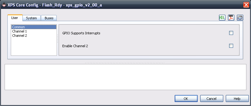
- Add an XPS_GPIO Core. In this case I have called it Flash_Rdy.
- Create the following External Ports
- Flash_RPN_pin, O
- Flash_CEN_pin, O
- Flash_OEN_pin, O
- Flash_WEN_pin, O
- Flash_DQ_pin, IO, [0:31]
- Flash_A_pin, O, [9:29]
- Flash_Rdy_pin, I
- Create the following connections between the 3 Cores & External Ports we just created.
- Connect Flash_Mem/Mem_A to Flash_A_Bus_Split/Sig
- Connect Flash_Mem/Mem_RPN to External Ports/Flash_RPN_pin
- Connect Flash_Mem/Mem_CEN to External Ports/Flash_CEN_pin
- Connect Flash_Mem/Mem_OEN to External Ports/Flash_OEN_pin
- Connect Flash_Mem/Mem_WEN to External Ports/Flash_WEN_pin
- Connect Flash_Mem/Mem_DQ to External Ports/Flash_DQ_pin
- Connect Flash_Rdy/GPIO_IO_I to External Ports/Flash_Rdy_pin
- Connect Flash_A_Bus_Split/Out1 to External Ports/Flash_A_pin
- The following image shows all of the connections between the External Ports, Flash_Mem (XPS_MCH_EMC), Flash_Rdy (UTIL_BUS_SPLIT), & Flash_Rdy (XPS_GPIO).
- In the Addresses tab, ensure that the Flash_Mem Size is set to 8M.
- The UCF file should include the following entries (your LOC values will be different).
- Note that the DQ pins are in reverse order when compared to the Atmel Flash datasheet. This must be done to overcome a Big Endian/Little Endian inconsistency between the Xilinx XPS_MCH_EMC and the Atmel Flash part. In this case, flash_DQ_pin<0 - 15> represents the "1st" flash part and flash_DQ_pin<16 - 31> represents teh "2nd" flash part.
- Note that the A pins are also in reverse order to overcome a Big Endian/Little Endian inconsistency.
- Net flash_DQ_pin<31> LOC=F24;
- Net flash_DQ_pin<30> LOC=F25;
- Net flash_DQ_pin<29> LOC=L17;
- Net flash_DQ_pin<28> LOC=L18;
- Net flash_DQ_pin<27> LOC=F23;
- Net flash_DQ_pin<26> LOC=E24;
- Net flash_DQ_pin<25> LOC=K18;
- Net flash_DQ_pin<24> LOC=K19;
- Net flash_DQ_pin<23> LOC=G22;
- Net flash_DQ_pin<22> LOC=F22;
- Net flash_DQ_pin<21> LOC=J20;
- Net flash_DQ_pin<20> LOC=J19;
- Net flash_DQ_pin<19> LOC=D26;
- Net flash_DQ_pin<18> LOC=E26;
- Net flash_DQ_pin<17> LOC=D24;
- Net flash_DQ_pin<16> LOC=D25;
- Net flash_DQ_pin<15> LOC=K26;
- Net flash_DQ_pin<14> LOC=K25;
- Net flash_DQ_pin<13> LOC=M22;
- Net flash_DQ_pin<12> LOC=M21;
- Net flash_DQ_pin<11> LOC=K22;
- Net flash_DQ_pin<10> LOC=K23;
- Net flash_DQ_pin<9> LOC=M18;
- Net flash_DQ_pin<8> LOC=M19;
- Net flash_DQ_pin<7> LOC=J22;
- Net flash_DQ_pin<6> LOC=J23;
- Net flash_DQ_pin<5> LOC=K21;
- Net flash_DQ_pin<4> LOC=L22;
- Net flash_DQ_pin<3> LOC=G24;
- Net flash_DQ_pin<2> LOC=G23;
- Net flash_DQ_pin<1> LOC=K20;
- Net flash_DQ_pin<0> LOC=L20;
- Net flash_A_pin<20> LOC=U20;
- Net flash_A_pin<19> LOC=V21;
- Net flash_A_pin<18> LOC=AA25;
- Net flash_A_pin<17> LOC=AA24;
- Net flash_A_pin<16> LOC=U18;
- Net flash_A_pin<15> LOC=U19;
- Net flash_A_pin<14> LOC=Y23;
- Net flash_A_pin<13> LOC=Y22;
- Net flash_A_pin<12> LOC=T20;
- Net flash_A_pin<11> LOC=U21;
- Net flash_A_pin<10> LOC=Y25;
- Net flash_A_pin<9> LOC=Y24;
- Net flash_A_pin<8> LOC=T17;
- Net flash_A_pin<7> LOC=T18;
- Net flash_A_pin<6> LOC=V22;
- Net flash_A_pin<5> LOC=W23;
- Net flash_A_pin<4> LOC=V25;
- Net flash_A_pin<3> LOC=V24;
- Net flash_A_pin<2> LOC=U22;
- Net flash_A_pin<1> LOC=V23;
- Net flash_A_pin<0> LOC=R20;
- Net flash_WEN_pin LOC=U23;
- Net flash_OEN_pin LOC=U24;
- Net flash_CEN_pin LOC=R19;
- Net flash_RPN_pin LOC=N21;
- Net flash_Rdy_pin LOC=P22;
- In your C code, when writing to the Flash memory the Address must be Left-Shifted 2 bits. Therefore your write data call should look something like this
- FLASH_ADDR is a pointer to the base address of the XPS_EMC_MCH.
- ui_waddr is the write address and is an Xuint32.
- ui_wdata is the write data and is an Xuint32.
- XGpio_WriteReg(FLASH_ADDR, ui_waddr << 2, us_wdata);;
- When reading from the Flash memory, the Address must again be Left-Shifted by 2 bits. Your read data call should look something like this
- FLASH_ADDR is a pointer to the base address of the XPS_EMC_MCH.
- ui_raddr is the write address and is an Xuint32.
- XGpio_ReadReg(FLASH_ADDR, ui_raddr << 2)


